USA/Canada:
Toll Free:
Europe:
(315) 432-8909
(800) 411-6596
+44 2392-232392
Available on Tape and
Reel for Pick and Place
Manufacturing.
Model BD4859N5050AHF
Rev A
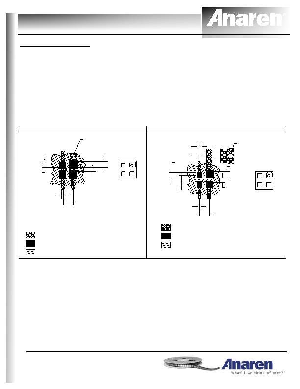
Mounting Configuration:
In order for Xinger surface mount components to work optimally, the proper impedance transmission lines must be
used to connect to the RF ports. If this condition is not satisfied, insertion loss, Isolation and VSWR may not meet
published specifications.
All of the Xinger components are constructed from ceramic filled PTFE composites which possess excellent electrical
and mechanical stability having X and Y thermal coefficient of expansion (CTE) of 17 ppm/
o
C.
An example of the PCB footprint used in the testing of these parts is shown below. An example of a DC-biased
footprint is also shown below. In specific designs, the transmission line widths need to be adjusted to the unique
dielectric coefficients and thicknesses as well as varying pick and place equipment tolerances
With No DC Bias
With DC Bias
Solder Resist
Footprint Pad (s)
Circuit Pattern
Dimensions are in Inches [Millimeters]
Mounting Footprint
Plated thru
hole to
ground
3X Transmission
Line
.020 [0.51]
.014 [0.36]
.008 [0.20]
3X
.011 [0.28]
SQ
Plated thru
hole to
ground
3X Transmission
Line
3X .011
[0.28]
3X .011
[0.28]
.020
[0.51]
.014 [0.36]
.008 [0.20]
.008 [0.20]
Solder Resist
Footprint Pad (s)
Circuit Pattern
Dimensions are in Inches [Millimeters]
.020 [0.51]
发布紧急采购,3分钟左右您将得到回复。
相关PDF资料
BICOLOG20100
ANTENNA ISOTROPIC 20MHZ-1GHZ RAD
CA9-9-D
CABLE DB9M-DB9F
CATTEN-0100
ATTENUATOR SMA 3GHZ 50 OHM 10DB
CATTEN-0150
ATTENUATOR SMA 3GHZ 50 OHM 15DB
CATTEN-01R0
ATTENUATOR SMA 3GHZ 50 OHM 1DB
CATTEN-01R5
ATTENUATOR SMA 3GHZ 50 OHM 1.5DB
CATTEN-0200
ATTENUATOR SMA 3GHZ 50 OHM 20DB
CATTEN-02R0
ATTENUATOR SMA 3GHZ 50 OHM 2DB
相关代理商/技术参数
BD4859N5075A00
制造商:ANAREN 制造商全称:Anaren Microwave 功能描述:Ultra Low Profile 0404 Balun 50ヘ to 75ヘ Balanced
BD4860
制造商:ROHM 制造商全称:Rohm 功能描述:Standard CMOS Voltage Detector IC
BD4860_09
制造商:ROHM 制造商全称:Rohm 功能描述:Standard CMOS Voltage Detector IC
BD4860FVE
制造商:ROHM Semiconductor 功能描述:IC,Reset IC,Vdetect=6.0V,OpenDrain,VSOF5
BD4860FVE-TR
功能描述:电压监测器/监控器 CMOS DETEC VOLT 2.5V RoHS:否 制造商:Texas Instruments 监测电压数:2 监测电压:Adjustable 输出类型:Open Drain 欠电压阈值: 过电压阈值: 准确性:1 % 工作电源电压:1.5 V to 6.5 V 工作电源电流:1.8 uA 最大工作温度:+ 125 C 封装 / 箱体:SON-6 安装风格:SMD/SMT
BD4860G
制造商:ROHM 制造商全称:Rohm 功能描述:Voltage Detector IC
BD4860G-TR
功能描述:电压监测器/监控器 CMOS DETEC VOLT 6.0V RoHS:否 制造商:Texas Instruments 监测电压数:2 监测电压:Adjustable 输出类型:Open Drain 欠电压阈值: 过电压阈值: 准确性:1 % 工作电源电压:1.5 V to 6.5 V 工作电源电流:1.8 uA 最大工作温度:+ 125 C 封装 / 箱体:SON-6 安装风格:SMD/SMT
BD487
制造商:INFINEON 制造商全称:Infineon Technologies AG 功能描述:PNP SILICON PLANAR TRANSISTORS
